TGV (Glass Substrate for Semiconductors)
The Dream Material, Carving Semiconductors into Glass.
Advanced TGV Glass Substrate Solutions Powered by Ultra-Precision Processing
Glass substrates are semiconductor bases made from glass, replacing conventional plastic materials. Applying glass instead of plastic allows for:
· Thinner semiconductor packages
· Up to 50% reduction in power consumption
· Significant improvement in data processing capabilities
JNTC possesses advanced technologies essential for glass-based semiconductor packaging, including:
· Glass cutting for substrate processing
· Laser Through Glass Via (TGV) formation
· Electrode plating for glass packaging substrates
| Property | Description | Glass | Organic | Silicon |
|---|---|---|---|---|
| Thermal resistance | Thermal stabililty | ◯ | ✕ | ◯ |
| Electrical Insulation | Prevents electrical signal interference |
◯ | △ | ✕ |
| Flatness | Mechanical stability (warpage) | ◯ | ✕ | ◯ |
| Surface Uniformity |
Suitable for etching and fine-pitch processing |
◯ | ✕ | ◯ |
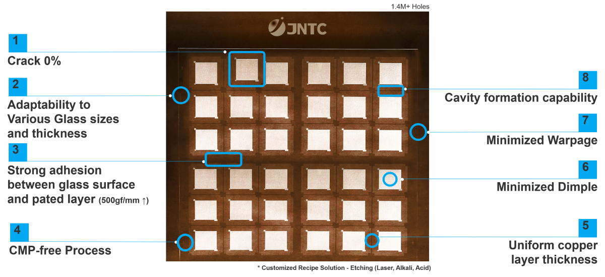
Core Value
Laser
Rapid Through-Glass via processing with
high-precision positioning
Etching
Consistent via
formation with
smooth surface finish
Metalizing
Achieves uniform plating surface with superior
adhesion strength (500gf/mm↑)
CMP-free
CMP-free, Process with uniform thickness, Simplified
workflow and cost reduction
JNTC TGV Key Values